|
 |
OLED [From Wikipedia, the free encyclopedia] |
|
 |
Analysis of OLED Thin Films – A Few Examples (Ref: Ellipso Technology) |
|
| |
|
|
 |
|
|
| |
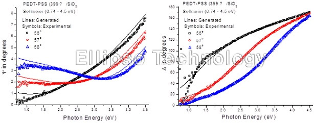
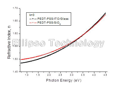
1-1. PEDT-PSS on SiO2 (Multiple AOI Ellipsometry) |
| |
 |
|
| |
Film : PEDT-PSS
Thickness = 39.9 nm
R.I. Dispersion (Sellmeier) |
| Substrate : SiO2 |
|
 |
|
|
| |
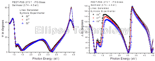
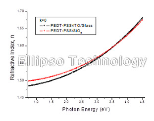
1-2. PEDT-PSS on ITO Coated Glass (Multiple AOI Ellipsometry) |
| |
 |
|
| |
Film : PEDT-PSS
Thickness = 37.3 nm
R.I. Dispersion (Sellmeier) |
| Substrate : ITO Coated Glass |
|
 |
|
|
|
 |
|
|
| |
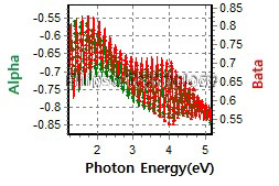
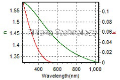
2-1. PEDOT/Hardcoating/Primer on PET |
| |
|
Thickness, PEDOT: 110.538 nm
Hardcoating : 2981.833nm
Primer : 96.676nm |
| R.I. Dispersion of PEDOT |
| Substrate : PET |
|
|
|
 |
|
|
| |
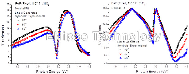
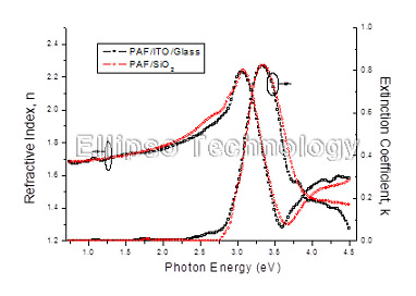
3-1. PAF on SiO2 (Multiple AOI Ellipsometry) |
| |
 |
|
| |
Film : PAF
Thickness = 110.7 nm
R.I. Dispersion (Sellmeier + n,k Inv.) |
| Substrate : SiO2 |
|
 |
|
|
| |
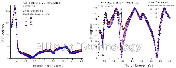
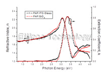
3-2. PAF on ITO Coated Glass (Multiple AOI Ellipsometry) |
| |
 |
|
| |
Film : PAF
Thickness = 101.0 nm
R.I. Dispersion (Sellmeier + n,k Inv.) |
| Substrate : ITO Coated Glass |
|
 |
|
|
|
 |
|
|
| |
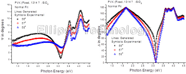
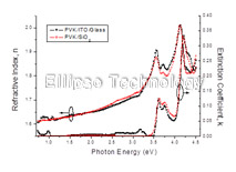
4-1. PVK on SiO2 Glass (Multiple AOI Ellipsometry) |
| |
 |
|
| |
Film : PVK
Thickness = 131.4 nm
R.I. Dispersion (Sellmeier + n,k Inv.) |
| Substrate : SiO2 |
|
 |
|
|
| |
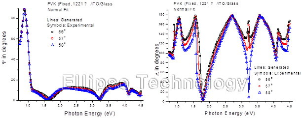
4-2. PVK on ITO Coated Glass (Multiple AOI Ellipsometry) |
| |
 |
|
| |
Film : PVK
Thickness = 122.1 nm
R.I. Dispersion (Sellmeier + n,k Inv.) |
| Substrate : ITO Coated Glass |
|
 |
|
|
|
 |
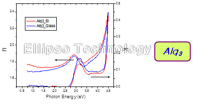
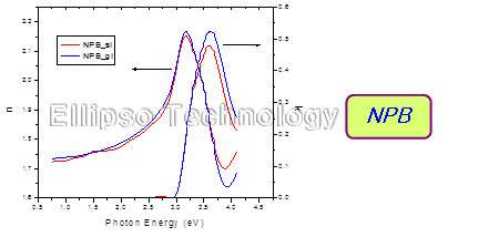
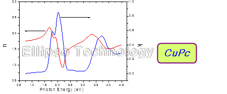
5. Complex Refractive Index of Alq3, NPB, CuPc |
[TOP] |
|
|
| |


 |
|
 |
|
|
| |
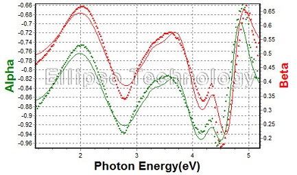
6-1. Alq3on c-Si |
| |
| Alq3 Thickness : 212.48 nm |
| R.I. (@633 nm) : 1.6877 |
| Substrate : Crystalline Silicon |
|
 |
|
|
|
 |
|
|
| |
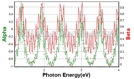
7-1. SiO2/GaN on Al2O3 |
| |
Thickness
SiO2 : 1091.99 nm
GaN : 4499.28 nm. |
| Substrate : Al2O3 |
|
 |
|
|
 |
|
|
| |
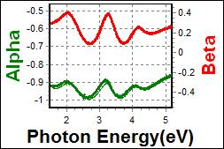
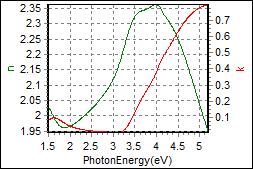
8-1. NPB/ITO on Glass |
| |
|
| Thickness, NPB: 56.399 nm |
| R.I. Dispersion of NPB |
| Substrate : Glass |
|
|
|
| |
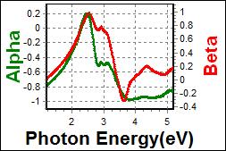
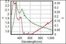
8-2. LCP180 on c-Si |
| |
|
| Thickness, LCP180: 70.055 nm |
| R.I. Dispersion of LCP180 |
| Substrate : c-Si |
|
|
|
| |
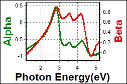
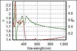
8-3. LHT001 on c-Si |
| |
|
| Thickness, LHT001: 62.485 nm |
| R.I. Dispersion of LHT001 |
| Substrate : c-Si |
|
|
|
| |
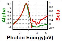
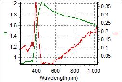
8-4. LPGH801 on c-Si |
| |
|
| Thickness, LPGH801 : 61.585 nm |
| R.I. Dispersion of LPGH801 |
| Substrate : c-Si |
|
|
|
| |
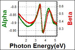
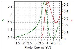
8-5. TPBi on Glass |
| |
|
| Thickness, TPBi : 101.149 nm |
| R.I. Dispersion of TPBi |
| Substrate : Glass |
|
|
|
| |
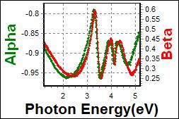
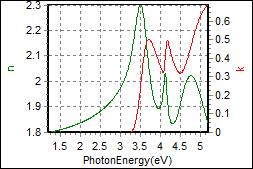
8-6. TcTa on Glass |
| |
|
| Thickness, TcTa : 93.090 nm |
| R.I. Dispersion of TcTa |
| Substrate : Glass |
|
|
|
| |
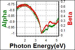
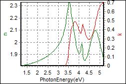
8-7. CBP/Primer on PET |
| |
|
| Thickness, CBP : 19.489 nm |
| R.I. Dispersion of CBP |
| Substrate : PET |
|
|
|
 |
|
|
| |
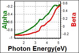
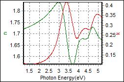
9-1. HTL0.5 on c-Si |
| |
|
| Thickness, HTL0.5x : 23.261 nm |
| R.I. Dispersion of HTL0.5 |
| Substrate : PET |
|
|
|
 |
|
|
| |
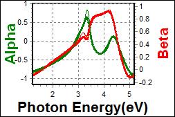
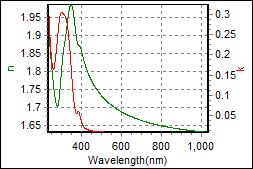
10-1. EML(Organic) on c-Si |
| |
|
| Thickness, EML : 53.232 nm |
| R.I. Dispersion of EML |
| Substrate : c-Si |
|
|
|
 |
|
|
| |
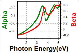
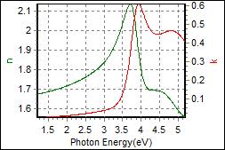
11-1. YEML 0.7 on c-Si |
| |
|
| Thickness, YEML0.7 : 33.700 nm |
| R.I. Dispersion of YEML0.7 |
| Substrate : c-Si |
|
|
|
 |
From Wikipedia, the free encyclopedia |
[TOP] |
|
|
 |
|
|
| |
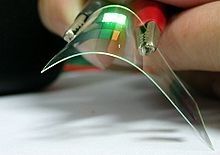 |
| Demonstration of a flexible OLED device |
|
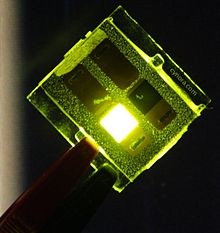 |
| A green emitting OLED device |
|
|
|
| |
An OLED (organic light-emitting diode) is a light-emitting diode (LED) in which the emissive electroluminescent layer is a film of organic compound which emit light in response to an electric current. This layer of organic semiconductor material is situated between two electrodes. Generally, at least one of these electrodes is transparent.
There are two main families of OLEDs: those based on small molecules and those employing polymers. Adding mobile ions to an OLED creates a light-emitting electrochemical cell or LEC, which has a slightly different mode of operation. OLED displays can use either passive-matrix (PMOLED) or active-matrix addressing schemes. Active-matrix OLEDs (AMOLED) require a thin-film transistor backplane to switch each individual pixel on or off, but allow for higher resolution and larger display sizes.
An OLED display works without a backlight. Thus, it can display deep black levels and can be thinner and lighter than a liquid crystal display (LCD). In low ambient light conditions such as a dark room an OLED screen can achieve a higher contrast ratio than an LCD, whether the LCD uses cold cathode fluorescent lamps or LED backlight. Due to its low thermal conductivity, an OLED typically emits less light per area than an inorganic LED.
OLEDs are used in television screens, computer monitors, small, portable system screens such as mobile phones and PDAs, watches, advertising, information, and indication. OLEDs are also used in large-area light-emitting elements for general illumination. |
|
 |
|
|
| |
 |
|
| |
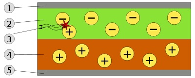
Schematic of a bilayer OLED: 1. Cathode (−), 2. Emissive Layer, 3. Emission of radiation, 4. Conductive Layer, 5. Anode (+)
A typical OLED is composed of a layer of organic materials situated between two electrodes, the anode and cathode, all deposited on a substrate. The organic molecules are electrically conductive as a result of delocalization of pi electrons caused by conjugation over all or part of the molecule. These materials have conductivity levels ranging from insulators to conductors, and therefore are considered organic semiconductors. The highest occupied and lowest unoccupied molecular orbitals (HOMO and LUMO) of organic semiconductors are analogous to the valence and conduction bands of inorganic semiconductors.
Originally, the most basic polymer OLEDs consisted of a single organic layer. One example was the first light-emitting device synthesised by J. H. Burroughes et al., which involved a single layer of poly(p-phenylene vinylene). However multilayer OLEDs can be fabricated with two or more layers in order to improve device efficiency. As well as conductive properties, different materials may be chosen to aid charge injection at electrodes by providing a more gradual electronic profile,[1] or block a charge from reaching the opposite electrode and being wasted.[2] Many modern OLEDs incorporate a simple bilayer structure, consisting of a conductive layer and an emissive layer. More recent developments in OLED architecture improves quantum efficiency (up to 19%) by using a graded heterojunction.[3] In the graded heterojunction architecture, the composition of hole and electron-transport materials varies continuously within the emissive layer with a dopant emitter. The graded heterojunction architecture combines the benefits of both conventional architectures by improving charge injection while simultaneously balancing charge transport within the emissive region.[4]
During operation, a voltage is applied across the OLED such that the anode is positive with respect to the cathode. A current of electrons flows through the device from cathode to anode, as electrons are injected into the LUMO of the organic layer at the cathode and withdrawn from the HOMO at the anode. This latter process may also be described as the injection of electron holes into the HOMO. Electrostatic forces bring the electrons and the holes towards each other and they recombine forming an exciton, a bound state of the electron and hole. This happens closer to the emissive layer, because in organic semiconductors holes are generally more mobile than electrons. The decay of this excited state results in a relaxation of the energy levels of the electron, accompanied by emission of radiation whose frequency is in the visible region. The frequency of this radiation depends on the band gap of the material, in this case the difference in energy between the HOMO and LUMO.
As electrons and holes are fermions with half integer spin, an exciton may either be in a singlet state or a triplet state depending on how the spins of the electron and hole have been combined. Statistically three triplet excitons will be formed for each singlet exciton. Decay from triplet states (phosphorescence) is spin forbidden, increasing the timescale of the transition and limiting the internal efficiency of fluorescent devices. Phosphorescent organic light-emitting diodes make use of spin–orbit interactions to facilitate intersystem crossing between singlet and triplet states, thus obtaining emission from both singlet and triplet states and improving the internal efficiency.
Indium tin oxide (ITO) is commonly used as the anode material. It is transparent to visible light and has a high work function which promotes injection of holes into the HOMO level of the organic layer. A typical conductive layer may consist of PEDOT:PSS[5] as the HOMO level of this material generally lies between the workfunction of ITO and the HOMO of other commonly used polymers, reducing the energy barriers for hole injection. Metals such as barium and calcium are often used for the cathode as they have low work functions which promote injection of electrons into the LUMO of the organic layer.[6] Such metals are reactive, so require a capping layer of aluminium to avoid degradation.
Single carrier devices are typically used to study the kinetics and charge transport mechanisms of an organic material and can be useful when trying to study energy transfer processes. As current through the device is composed of only one type of charge carrier, either electrons or holes, recombination does not occur and no light is emitted. For example, electron only devices can be obtained by replacing ITO with a lower work function metal which increases the energy barrier of hole injection. Similarly, hole only devices can be made by using a cathode comprised solely of aluminium, resulting in an energy barrier too large for efficient electron injection.[7-9]
- Piromreun, Pongpun; Oh, Hwansool; Shen, Yulong; Malliaras, George G.; Scott, J. Campbell; Brock, Phil J. (2000). "Role of CsF on electron injection into a conjugated polymer". Applied Physics Letters 77 (15): 2403. doi:10.1063/1.1317547.
- D. Ammermann, A. Böhler, W. Kowalsky, Multilayer Organic Light Emitting Diodes for Flat Panel Displays, Institut für Hochfrequenztechnik, TU Braunschweig, 1995.
- "Organic Light-Emitting Diodes Based on Graded Heterojunction Architecture Has Greater Quantum Efficiency". University of Minnesota. http://www.license.umn.edu/Products/Organic-Light-Emitting-Diodes-Based-on-Graded-Heterojunction-Architecture-Has-Greater-Quantum-Efficiency__20100200.aspx. Retrieved 31 May 2011.
- Holmes, Russell; Erickson, N. (27). "Highly efficient, single-layer organic light-emitting devices based on a graded-composition emissive layer". Applied Physics Letters 97: 083308. http://apl.aip.org/resource/1/applab/v97/i8/p083308_s1.
- Carter, S. A.; Angelopoulos, M.; Karg, S.; Brock, P. J.; Scott, J. C. (1997). "Polymeric anodes for improved polymer light-emitting diode performance". Applied Physics Letters 70 (16): 2067. doi:10.1063/1.118953.
- Friend, R. H.; Gymer, R. W.; Holmes, A. B.; Burroughes, J. H.; Marks, R. N.; Taliani, C.; Bradley, D. D. C.; Santos, D. A. Dos et al (1999). Nature 397 (6715): 121. doi:10.1038/16393.
- Davids, P. S.; Kogan, Sh. M.; Parker, I. D.; Smith, D. L. (1996). "Charge injection in organic light-emitting diodes: Tunneling into low mobility materials". Applied Physics Letters 69 (15): 2270. doi:10.1063/1.117530.
- Crone, B. K.; Campbell, I. H.; Davids, P. S.; Smith, D. L. (1998). "Charge injection and transport in single-layer organic light-emitting diodes". Applied Physics Letters 73 (21): 3162. doi:10.1063/1.122706.
- Crone, B. K.; Campbell, I. H.; Davids, P. S.; Smith, D. L.; Neef, C. J.; Ferraris, J. P. (1999). "Device physics of single layer organic light-emitting diodes". Journal of Applied Physics 86 (10): 5767. doi:10.1063/1.371591
|
|
